

3D model · revision 0.1
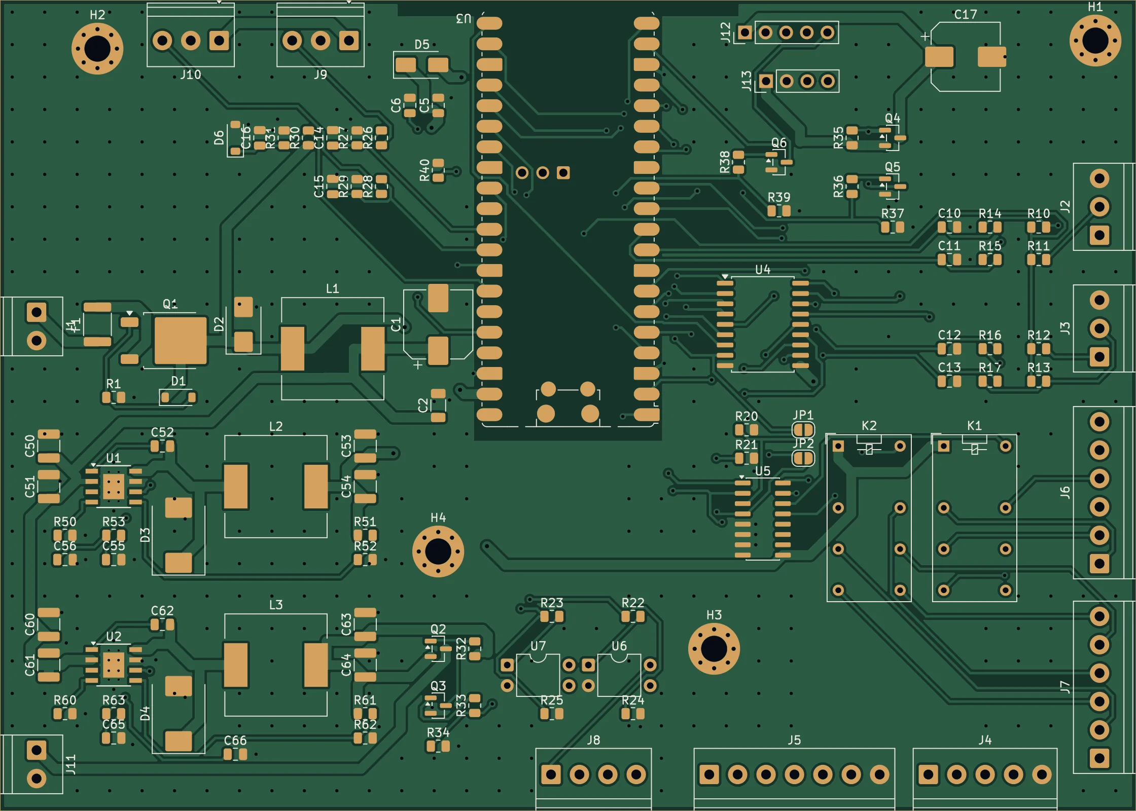
The Pico 2 W controller board in 3D
Rotate the board, zoom in and pick a block to see what it does and what it is made of. The model comes straight from the KiCad project: the same footprints, traces and designators as in the manufacturing files.
This is a design, not a photo of a finished unit: the revision 0.1 board has not been ordered yet. Before ordering, a prototype has to confirm Bluetooth in two roles, TLS 1.3 over the modem and the WireLink channel on mbedTLS.
The board in numbers
- Size
- 140 × 100 × 1.6 mm
- Layers
- 2, ground pour on both sides
- Parts to populate
- 96 (48 BOM lines)
- ERC / DRC
- 0 errors
What’s on the board
01Raspberry Pi Pico 2 W
The brain of the board: an RP2350 with 520 KB of SRAM and 4 MB of flash plus a CYW43439 radio (Wi-Fi and Bluetooth LE). The module is soldered by its castellated edges, without pin headers, so it copes better with vibration in the car. It sits at the top edge, turned so that the antenna is on the board edge with no copper underneath. Flashing and debugging go through the Pico's own USB.
- Chip: RP2350 + CYW43439
- Supply: VSYS from the 5 V logic rail via an SS34 Schottky (D5)
- Analog ground: AGND tied to GND through 0 Ω (R40)
Parts: U3, D5, C5, C6
0212 V input and protection
Permanent 12 V from the car goes through four stages: a polymer fuse, reverse-polarity protection on a P-MOSFET, a TVS diode for load dump and an LC filter. Only after them come the converters and the 12 V feed for the ULN drivers.
- Fuse: polymer 3 A / 33 V, 1812 (F1)
- Reverse polarity: SQD50P06-15L, −60 V (Q1), 15 V Zener on the gate (D1)
- Transients: SMBJ24A TVS (D2), about 39 V at load dump
- Filter: 10 µH / 4 A (L1) + 100 µF 50 V and 1 µF
- Connector: J1 — 12 V and ground
Parts: J1, F1, Q1, D1, R1, D2, L1, C1, C2
03Converter A — 5 V logic
A switching converter rated for up to 60 V in. The margin comes from the TVS diode: it clamps load dump at about 39 V, which ruled out 36 V and 40 V parts. This rail feeds the Pico, the current-sense modules and — through its own switch — the modem.
- Output: 5 V, up to 3.5 A
- Frequency: about 600 kHz (RT 162 kΩ)
- FB divider: 31.6 kΩ / 6.04 kΩ 1%
- Inductor and diode: 8.2 µH (L2), B560C 60 V 5 A (D3)
- Capacitors: input 2 × 2.2 µF 100 V, output 2 × 47 µF
Parts: U1, L2, D3, C50, C51, C52, C53, C54, C55, C56, R50, R51, R52, R53
04Converter B — 5 V LED strip
A second, identical converter just for the LED strip, so a current spike from the strip cannot drag the logic rail down.
- Output: 5 V, up to 3.5 A
- Parts: same as rail A: L3 8.2 µH, D4 B560C
Parts: U2, L3, D4, C60, C61, C62, C63, C64, C65, C66, R60, R61, R62, R63
05LED strip output
The strip gets 5 V from converter B through a high-side switch controlled by the Pico. During a long stop the strip is cut off entirely and draws nothing from the battery.
- Switch: AO3401A P-MOSFET (Q2) + MMBT3904 (Q3)
- Control: GP22, 100 kΩ pull-down
- Connector: J11 — 5 V and ground
Parts: J11, Q2, Q3, R32, R33, R34
06Door lock inputs
Four signals from the Golf IV's factory locks: latch position and door state, for the driver's and passenger's side. The lock contact pulls the line to chassis ground. Each line has a pull-up to 3.3 V, a series resistor and a capacitor — the filter absorbs spikes from the lock motors and the resistor limits current during transients.
- Lines: GP6–GP9 (lock pins 5 and 8)
- Filter: 2.2 kΩ to 3.3 V, 10 kΩ series, 100 nF (τ ≈ 1 ms)
- In firmware: 50 ms debounce
Parts: J2, J3, R10, R11, R12, R13, R14, R15, R16, R17, C10, C11, C12, C13
07Windows and mirrors
Darlington drivers wired in parallel with the factory buttons — the board 'presses' them the way the driver would. COM goes to 12 V after the protection stage, so the flyback diodes are inside the chips. Control inputs have external 100 kΩ pull-downs (RP2350 erratum E9) so nothing is pressed after reset.
- ULN2803A: windows up/down ×2, mirror: select L/R, up, down (GP10–GP17)
- ULN2003A: mirror left/right (GP18, GP19) + K1/K2 coils
- Connectors: J4 — windows (4 + ground), J5 — mirrors (6 + ground)
Parts: U4, U5, J4, J5
08Mirror relays (optional)not populated
Footprints for two DPDT relays that reverse the polarity of the mirror motors. They get populated only if the Golf IV mirror switch needs it — still to be checked against the car's wiring diagram. That's why they are translucent in the model.
- Relay: Omron G5V-2, 12 V coil
- Control: ULN2003A ch. 3–4 via JP1/JP2 jumpers
- Contacts: J6, J7 — 6 terminals each
Parts: K1, K2, J6, J7, JP1, JP2, R20, R21
09Central-lock remote
Two optocouplers 'press' the buttons of a spare central-lock remote: lock and unlock. The remote stays galvanically isolated from the board.
- Control: GP20, GP21 → 330 Ω → PC817 LED
- Pulse: 400 ms
- Connector: J8 — collector/emitter ×2
Parts: U6, U7, R22, R23, R24, R25, J8
10Sensing: window current and battery
The RP2350's built-in ADC measures the window motor current and the battery voltage — no separate ADC chip. The ACS712 current sensors are modules in the window harness; the board only carries their connectors and the dividers right next to the Pico pins.
- Window current: ACS712-20A, 10 k / 20 k divider → max 3.0 V (GP26, GP27)
- Battery: 100 k / 22 k 1%: 16 V → 2.9 V (GP28)
- Filter: 100 nF on each input; Zener D6 not populated
Parts: J9, J10, R26, R27, R28, R29, C14, C15, R30, R31, C16, D6, R40
11LTE modem header
The modem is a separate module; the board gives it a UART, power and the power-on key. When the car is parked the Pico cuts the modem's 5 V to spare the battery.
- UART0: GP0/GP1 — AT commands and PPP
- Power: AO3401A switch (Q4) from GP3, 220 µF at the header
- PWRKEY: MMBT3904 open collector (Q6) from GP2
Parts: J12, Q4, Q5, Q6, R35, R36, R37, R38, R39, C17
12Pi Zero 2 W header (plan B)not populated
A spare UART header in case the Pico can't handle Bluetooth in two roles at once or TLS 1.3 over PPP. A Pi Zero 2 W would then sit alongside and the board stays unchanged.
- Signals: UART1 (GP4/GP5), 5 V, ground
Parts: J13